Contactless temperature measurement of silicon wafer
A non-contact temperature measurement technology for silicon wafer under processing, with high accuracy, fast acquisition speed, and a large measurement range using a all-fiber cost-effective supercontinuum source.
Cite
Share
Technology at a glance
Specifications
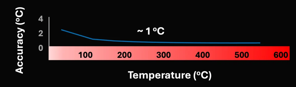
• High measurement accuracy: ~1 °C.
• Large measurement range: 30-550 °C.
• Fast measurement speed: ~66 ms.
• Multi-point measurement.
Architecture
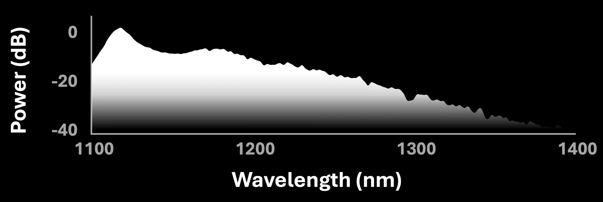
• All-fiber, cost-effective telecom-fibersupercontinuum source based measurement.
• Custom spectral shape (power spectral density drops exponentially towards longer wavelengths) to achieve high measurement accuracy with large measurement range.
×
How to Cite
Research outputs
Contactless temperature measurement of an in-process silicon wafer using a spectrally shaped supercontinuum source